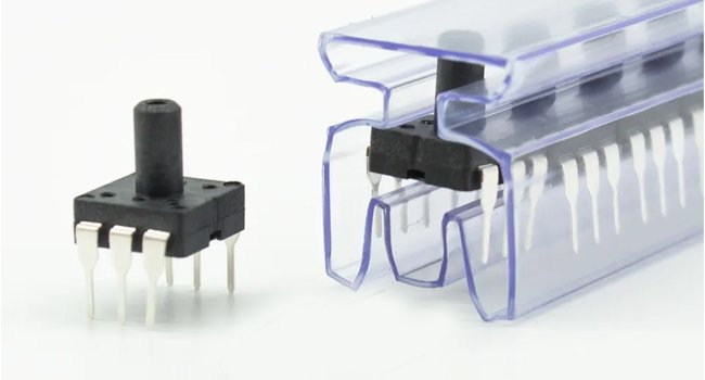
Engineers obsess over layout and Wheatstone bridges — yet package residual stress is what actually decides whether the same die delivers lab-grade stability or field-grade drift. Six dimensions, from silicon-cup etching to future co-design trends.
In industrial automation, automotive TPMS and fuel systems, aerospace, wearables, precision instruments, and oil & gas, silicon-piezoresistive MEMS pressure sensors dominate low- to high-pressure measurement. Mature microfabrication, high sensitivity, tiny size, fast dynamic response, low cost, and easy integration made them the default choice. But identical dies — same process, same layout — can differ by multiples, even an order of magnitude, in zero drift, thermal drift, long-term stability, repeatability, and hysteresis after different packaging. That gap is package stress.
Where Package Stress Comes From
At the device level, performance ceilings are set by the piezoresistive effect of single-crystal silicon, the geometry of the silicon-cup elastic membrane, and Wheatstone-bridge matching. In practice, however, batch tests and long-term aging show that packaging choices dominate finished-sensor error. Most hardware and mechanical engineers debugging thermal drift, zero shift, stability loss, or output jumps start with layout, resistor matching, temperature-compensation algorithms, and analog front-end tuning — and miss residual package stress, thermal-mismatch stress, and parasitic structural stress entirely.
Packaging is not mere physical protection and electrical breakout. It is the step that finalizes device performance, locks in reliability, and determines long-term stability. Parasitic stress couples into the sensing membrane together with the measured pressure, producing systematic error that ordinary circuit compensation cannot fully cancel.
Thermal-expansion mismatch is the root; process parasitics are the accelerants
The sensing element is an anisotropically wet-etched silicon-cup membrane. Single-crystal silicon has a diamond lattice; atomic density and bonding differ strongly by crystal plane, so alkaline etchants attack planes at strictly different rates. The (111) plane etches almost not at all and acts as a natural etch-stop sidewall — which is why the cup forms a clean inverted truncated pyramid. Industrial force sensors universally use (100) wafers with square etch windows; sidewalls land near the theoretical (100)/(111) angle.
Production uses P-ED etchant with a glass-reflux constant-temperature bath: about 1.2 µm/min at 95 °C and 1.5 µm/min at 100 °C. Etch time sets membrane thickness precisely. Dual-layer passivation keeps the diaphragm smooth and the sidewalls uniform, so mechanical properties are consistent at the die source. Ion implantation and diffusion then form four matched piezoresistors into a closed Wheatstone bridge. External pressure deflects the membrane; tensile and compressive zones change resistance differentially; the bridge outputs a voltage linear with pressure. Extreme mechanical strain sensitivity is both the advantage and the reason packaging stress is so damaging.
The core source of package stress is CTE mismatch across stacked materials. Silicon sits near 2.6 ppm/K. FR-4 substrates, epoxy molding compounds (EMC), die-attach silicones, metal headers, and solders expand far more. Through cure, temperature cycling, and field temperature swings, layers expand and contract unequally and constrain each other, generating interfacial shear, peel, and bending — package residual stress.
That parasitic stress does not care about signal origin. It superimposes on the membrane, causing passive bending, zero offset, thermal zero drift, and sensitivity drift. Because adhesives and polymers creep, residual stress relaxes slowly over time — long-term zero wander and aging. And because stress itself is temperature-dependent, a temperature–stress coupling error widens full-range measurement uncertainty.
Beyond CTE mismatch, the packaging flow injects multiple parasitics: die-attach cure residual stress, epoxy potting shrinkage, ultrasonic bond-pad crush, silicone-oil thermal expansion in oil-filled cans, and assembly preload. They couple and multiply the complexity of the error signature.
Three Mainstream Package Families
Depending on environment, accuracy, reliability grade, and cost, industrial silicon-piezoresistive sensors standardize into three families: epoxy plastic, metal oil-isolated, 그리고 ceramic hermetic. Their stress mechanisms, performance ceilings, failure modes, and fit-for-use differ sharply.
1. Epoxy plastic (EMC) packaging
Lowest cost, highest throughput, most mature — used in consumer electronics, appliances, and general industrial control. EMC encapsulation needs no hermetic seal and suits high-volume automated molding.
Low-stress EMC design is clear in principle: spherical fused/crystalline silica fillers shrink CTE toward silicon; polysiloxane or PBA/PMMA core–shell elastomers lower modulus and improve stress relaxation; coupling agents protect the interface from delamination and passivation cracks.
But epoxy has a glass-transition temperature. Below Tg, chain segments freeze and cure strain cannot relax — stress stays locked on the die. There is also a process trade-off: more filler lowers CTE but raises modulus (worse thermal stress); more elastomer softens the body but hurts strength, heat resistance, and insulation. High-quality plastic-packaged sensors typically serve −20 °C to moderate ranges with limited hermeticity and medium thermal drift — fine for civil use, not for harsh corrosive or aerospace duty.
2. Metal oil-isolated packaging
For chemical, oil & gas, automotive powertrain, and wide-temperature fluid sensing, the industry isolates the die from the medium with a stainless corrugated diaphragm and incompressible silicone oil.
Pressure acts on the corrosion-resistant stainless diaphragm; high-purity low-compressibility silicone oil transfers it almost losslessly to the die membrane, so the die never touches acid, alkali, oil, or moisture. Stress complexity rises, though: diaphragm thickness/corrugation geometry sets transfer uniformity and preload; die-attach modulus trades isolation against vibration robustness; poorly degassed oil injects huge extra stress when heated; oil thermal expansion itself needs cavity compensation.
Optimized industrial metal-isolated sensors deliver excellent zero temperature error and lineality across roughly −40 °C to elevated ranges, work with 316L-compatible corrosive media, and survive 108+ pressure cycles — the mainstream choice for high-accuracy industrial measurement.
3. Ceramic hermetic packaging
High reliability, low stress, excellent hermeticity — for precision industrial, aerospace, defense, and metrology. Alumina (6–8 ppm/K), aluminum nitride (5.1 ppm/K), and silicon nitride (2.8 ppm/K) match silicon far better than FR-4. Measured interfacial stress example: FR-4 attach ≈ 11.97 MPa shear / 15.2 MPa normal; alumina ceramic ≈ 7.28 MPa / 8.92 MPa.
Two process branches: soft attach (conductive adhesive / glass frit — mild, controllable stress) and hard seal (anodic bonding, Si–Si bonding — no adhesive, covalent interface). Anodic bonding of silicon to borosilicate glass is the workhorse for absolute-pressure vacuum reference cavities.
Swipe horizontally to view all columns →
| 패키지 | CTE match | Stress level | Typical use | Main limit |
|---|---|---|---|---|
| Epoxy plastic | Poor | High residual / Tg freeze | Consumer, appliances, general industrial | Weak hermeticity, medium drift |
| Metal oil-isolated | Complex / multi-body | Medium–high, coupled | Chemical, auto, oil & gas, wide T | Oil/diaphragm design critical |
| Ceramic hermetic | 훌륭한 | Low (esp. anodic bond) | Aerospace, defense, metrology | Cost above plastic |
Low-Stress Path: Materials · Process · Structure
FEA and experiments agree: package stress cannot be abolished by one lever. You need coordinated optimization of materials, process, and structure — suppress at the source, relax in-process, isolate along the path.
Materials: shrink mismatch, lower modulus
Substrate selection follows “CTE nearest match”: silicon nitride → aluminum nitride → alumina → FR-4. For high-stability devices, prioritize Si₃N₄ / AlN. Civil cost-optimized designs often settle on alumina.
Adhesives need trade-offs. Low-modulus, low-temperature acrylics or modified epoxies (cure as low as ~100 °C, modulus down to ~0.1 GPa) cut residual and thermal stress, but have poor thermal/electrical conductivity. High-reliability paths use Au–Sn / Au–Ge eutectics — strong and heat-tolerant, but high modulus demands strict CTE matching. Inside EMC, high spherical filler + core–shell elastomer + polysiloxane is the low-stress recipe. For metal oil cans, do not over-soften die attach (vibration risk); oil must be high-temperature vacuum degassed.
Process: suppress cure stress, enable relaxation
Most residual stress is born in attach cure and cool-down. Two frontier approaches:
- Rapid / pulsed local die heating (RDH) — short pulses heat only die + adhesive while the substrate stays cooler, cutting thermal mismatch and die warp by >50% (Fig. 9). Powerful but equipment-heavy.
- Thermal-cycle annealing — for specialty systems (e.g., silver-glass), cyclic heat treatment relaxes adhesive residual stress; material scope is limited.
Also critical: tune ultrasonic power / force / time on bonding; plasma-clean interfaces; control potting thickness and cure rate; and strictly manage vacuum fill / degas time for oil packages.
Structure: cut the stress path
Structural isolation is the most production-friendly lever today — high cost-performance without rewriting materials or process.
- Reduce die-attach area. Full-area attach couples substrate warp into the die. Smaller attach windows block the path; gyroscope resonance drift can drop >80%. (Fig. 10)
- Stress-compensation substrates. Elastic recessed substrates generate counter-moments under temperature change. Reported package output error can fall dramatically versus uncompensated designs. (Fig. 11)
- Compliant metal interposers. A flexible intermediate layer absorbs CTE mismatch; die warp can drop ~5×.
- Double-sided bond-wire suspension. Wires alone hold the die — nearly decoupled from substrate stress, but hard to mass-produce. (Fig. 12)
- Silicon pedestal isolation. Mount the sensitive die on a same-material silicon pedestal first, then assemble the pedestal into the can. Same-material matching isolates package/substrate parasitics; long-term drift can fall >75% with excellent cost-performance.
Compensation and Engineering Evaluation
Because residual stress remains temperature-dependent and creep-active, low-stress packaging must be paired with compensation, modeling, and verification.
- Analog resistor compensation — shunt a large compensation resistor Rp on one bridge arm under constant-current drive to cancel zero TCD; bridge-external resistors handle sensitivity TCD. Simple and production-friendly, but limited precision.
- Digital smart compensation — an on-board MCU samples output across temperature and applies multi-dimensional stress–temperature–error models. Higher accuracy at higher cost/complexity.
- Fast reliability screening — temperature coefficient strongly correlates with long-term stability, so TCD measurement can screen weak units without full aging.
- FEA in development — ANSYS-class tools predict stress distribution vs. substrate, adhesive modulus, attach area, and thermal cycling; cut physical iterations. Physical temperature cycling, pressure cycling, and aging remain mandatory to validate simulations.
Challenges and Future Directions
Low-stress packaging has matured, but real constraints remain: soft materials often sacrifice strength, thermal conductivity, or heat resistance; high-performance isolation structures are complex and costly for high-volume civil products. Many lab winners never convert to production.
Two main directions lead the next generation:
- New packaging materials — adhesives that combine low modulus, high heat resistance, and high thermal conductivity; substrates with silicon-like CTE at acceptable cost.
- Production-ready stress decoupling structures — simpler geometry that blocks stress transfer without inflating process difficulty.
Alongside those, package–chip co-design is becoming the default: packaging stress is considered while the sensing structure is still being designed, not after tape-out. Combined with digital temperature compensation, a materials–structure–algorithm stack balances cost, performance, and reliability across consumer, industrial, and aerospace tiers.
Many engineers pour every hour into layout and bridge matching while ignoring the package. The same silicon, packaged poorly, will never reach its design precision.
참조
- Wu Z., Yang S., Wu G. Low-stress packaging technology for MEMS devices. Micro-Nano Electronics and Intelligent Manufacturing, 2020, 2(04): 44–51. (in Chinese)
- Wang J. Packaging research of silicon piezoresistive pressure sensors. M.S. thesis, Hangzhou Dianzi University, 2015. (in Chinese)
- Li D., Ohlckers S. A., Fung C. D., et al. Stress-isolation packaging of silicon pressure sensors. In: National Conference on Sensors & Transducers, Chinese Institute of Electronics, 1994.
- Hou Q., Huang Y., Yu Y. Low-stress technology for epoxy molding compounds. China Plastics, 1999, 13(10): 6–10.
- Huang J., He M., Gao C., et al. Simulation of potting process effects on ceramic-isolated package bond pads. Modern Electronics Technique, 2022, 45(10): 5–9.
- Wang W., Qiao J., Liu X. Design of K05 high-pressure piezoresistive sensor. In: National Conference on Sensors & Transducers, 1987.
- Wang D. Stability of silicon piezoresistive force-sensitive devices and sensors. In: National Conference on Sensors & Transducers, 1994.
- Li G., Tseng A. Low stress packaging of a micromachined accelerometer. IEEE Trans. Electronics Packaging Manufacturing, 2001, 24(1): 18–25.
- Marinis T., Soucy J., Hanson D. Isolation of MEMS devices from package stresses by use of compliant metal interposers. In: 56th ECTC, IEEE, 2006: 1108–1117.
- Schröder S., Niklaus F., Nafari A., et al. Stress-minimized packaging of inertial sensors by double-sided bond wire attachment. J. Microelectromech. Syst., 2015, 24(4): 781–789.
- Walwadkar S., Farrell P., Felton L., et al. Effect of die-attach adhesives on stress evolution in MEMS packaging. In: SPIE Int. Symp. Microelectronics & MEMS, 2003: 847–852.
- Frutschy K., Rangaraj S., Dias R. Rapid die heating for low-stress die attach. IEEE Trans. Electronics Packaging Manufacturing, 2004, 27(2): 153–162.
- Suhir E. Thermal stress in microelectronics and photonics systems: review. J. Electronic Packaging, 2001, 123(4): 341–352.