Каталог
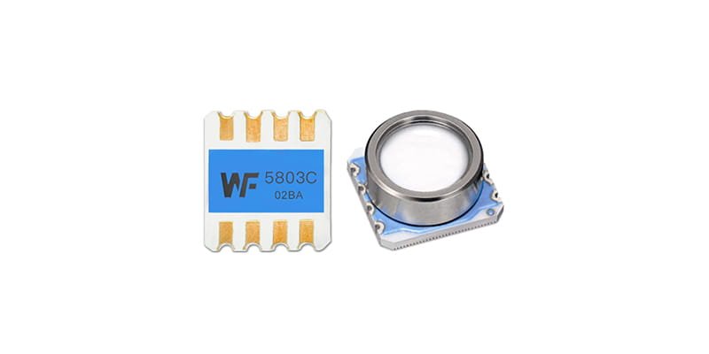
High-resolution sensing is not achieved solely by high-resolution digital output; it is the result of the joint action of MEMS mechanical design, front-end electronics, temperature compensation, and packaging. The WF282A-type sensor in the image shows common SMD package features: a metal top cover provides shielding and stability, a vent hole ensures reference contact with ambient air, and rear metal pads enable low-impedance connections. Understanding these physical factors helps maximize a sensor’s effective resolution at the system level.
1. Sensitivity and Dynamic Response
High sensitivity comes from geometric optimization of the MEMS cavity and strain structures, high-gain amplification of capacitive or resistive bridge circuits, and matching with low-noise amplifiers. Improving sensitivity requires trade-offs among bandwidth, linear range, and noise: increasing gain makes small changes more detectable but can also amplify thermal noise or process drift. Design must be guided by the target measurement bandwidth and the minimum detectable pressure difference; choose appropriate bridge topology, front-end amplifier, and filtering strategies to ensure real-time response and stable readings.

2. Noise Floor and Signal Integrity
The fundamental limit of high resolution is the noise floor: thermal noise, 1/f noise, and power-supply interference can mask weak signals. At the device level, using low-resistance bridges, optimized doping, and package shielding reduces thermal noise; at the circuit level, low-noise amplifiers, differential measurement, and careful ground routing reduce interference. Systems must pay attention to bandwidth limiting and filter design to lower noise without losing the signal details of interest, thereby effectively improving usable resolution.
3. Temperature Effects and Compensation Strategies
Temperature drift significantly affects high-resolution measurements: material thermal expansion, changes in semiconductor parameters, and packaging stress introduce offset and gain errors. Effective methods include integrating on-chip temperature sensing for real-time compensation, using dual-bridge or self-calibrating circuit designs, and applying calibration curves and multi-point linearization algorithms at the firmware level. Good thermal design and temperature compensation balance long-term stability with short-term sensitive capture, avoiding frequent manual intervention.
4. Packaging, Mechanical Stress, and Environmental Coupling
Packaging not only protects the die but directly affects sensing performance. A metal top cover and vent hole offer shielding and reference contact, but packaging stress, soldering processes, or adhesive intrusion can introduce mechanical bias. To maintain high resolution, select low-stress packaging materials, optimize pad layout, and design stress-isolation areas on the PCB. Additionally, consider humidity, vibration, and shock interference on micro-pressure detection and implement appropriate protection and filtering measures.
5. Calibration, Testing, and System Integration
Calibration strategy determines the actual usable resolution. High-resolution devices require multi-point calibration, noise measurements, and long-term drift tracking. Testing should include static noise spectrum, temperature-drift curves, and dynamic step response to verify target performance. At the system integration level, using differential measurement, digital filtering, and adaptive thresholds ensures robust detection of tiny pressure changes in the application, reducing false alarms and response delays.
Заключение
Starting from the angle of “high-resolution sensors sensitively capturing tiny pressure changes,” optimization must be carried out collaboratively across device design, front-end electronics, temperature compensation, packaging reliability, and calibration procedures. Only by controlling noise, stress, and drift across the entire chain can a system convert a sensor’s nominal resolution into practical, usable measurement sensitivity that meets engineering requirements for precise micro-pressure detection.
Вышеупомянутое введение лишь поверхностно коснулось области применения технологии датчиков давления. Мы продолжим изучать различные типы сенсорных элементов, используемых в различных продуктах, их работу, их преимущества и недостатки. Если вам нужна более подробная информация о том, что здесь обсуждается, вы можете просмотреть соответствующий контент далее в этом руководстве. Если у вас мало времени, вы также можете нажать здесь, чтобы загрузить подробную информацию об этом руководстве. Данные датчика давления воздуха PDF.
Для получения дополнительной информации о других сенсорных технологиях, пожалуйста, Посетите нашу страницу датчиков.