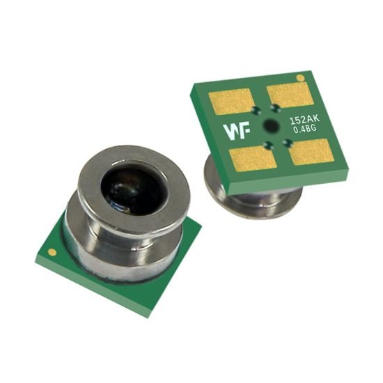
The heart of lowering packaging stress in MEMS devices is managing thermo-mechanical mismatch. By innovating across three dimensions — materials, processes and structures — you can strike the best balance between performance, reliability and cost, ensuring low-power sensors remain stable in mass production and over time.
Каталог
1. Problem background: why packaging stress determines device
surface and negative-pressure sensors are especially sensitive
Packaging is a major factor in MEMS commercialisation: it can account for the lion’s share of product cost, and many reliability issues trace back to packaging. Residual thermal stress introduced during packaging causes chip warpage, offset drift and frequency shifts — problems that hit piezoresistive and resonant elements hard. For surface-pressure and negative-pressure sensors, tiny mechanical deformations change calibration and affect measurement accuracy and power-management strategies. Waterproof surface-pressure sensors must balance sealing and stress control. So, consider packaging stress from product definition onward, and weigh it against the device’s operating temperature and long-term stability requirements.

2. Stress generation mechanism (theoretical model and key parameters)
three-layer model gives a quantitative view — ΔT, Δα and material stiffness
You can quantify packaging stress with a chip–glue–substrate three-layer model. The main drivers are the difference between cure temperature and operating temperature (ΔT), and the mismatch in coefficients of thermal expansion (Δα) between chip and substrate. The Young’s modulus and thickness of each layer also shape the stress level. When the adhesive cures and the assembly cools, thermal mismatch induces bending in the thin silicon die, producing shear and peel stresses; these in turn relate to bond area and constraints. Running calculations on these parameters lets you estimate offset drift and interface fracture risk, which cuts down trial-and-error during development.
3. Material optimisation paths
choose low modulus, low-cure adhesives and substrates that match silicon’s CTE — but watch thermal and electrical needs
Material choices aim to lower the adhesive’s Young’s modulus and cure temperature to reduce residual thermal stress. Typical approaches include low-temperature curing, low-modulus epoxies or adding flexible metal interlayers. For substrates, pick materials with a CTE close to silicon — specialised ceramics or metal-ceramic composites are common choices. However, there are trade-offs: low-modulus epoxies usually have poor thermal and electrical conductivity, which is a problem in high-power or EMI-sensitive designs; low-CTE substrates tend to be costly and harder to manufacture. So, for surface-pressure, negative-pressure and waterproof surface-pressure sensors, establish material priorities and tolerance levels based on functional needs.
4. Process optimisation methods
precise thermal control and staged stress relaxation are practical ways to cut
On the process side, local heat pulsing and thermal cycling during cure can lower the net temperature mismatch. Local rapid heating targets the die and adhesive while keeping the substrate cooler, reducing instantaneous ΔT; thermal cycling leverages the adhesive’s viscoelastic relaxation to release stress progressively. These methods can notably reduce warpage and frequency drift, but they add process complexity and cost, and they’re only suitable for certain adhesive systems. In production, these process tweaks are usually combined with material and structural measures to hit acceptable stress levels without blowing the budget.
5. Structural solutions (reduce bond area and isolate stress)
mechanical design to break stress paths is often the most effective, scalable
Structurally, reducing bond area, adding stress-compensation cavities or inserting flexible interlayers between die and rigid substrate can dramatically cut die deformation. Shrinking bond area shortens stress transfer paths; stress-compensation structures generate counteracting stress to cancel thermal stress; flexible metal interlayers act as cushions between silicon and stiff substrates. Wire-bonded, adhesive-free approaches (dual-side bond wires) can almost eliminate adhesive-transmitted stress, though they’re more complex to manufacture. Structural optimisation usually achieves the best balance between performance and manufacturability and is widely used in volume production.
Заклучок
To lower packaging stress in MEMS devices you must tackle materials, processes and structures together and make practical trade-offs. For low-power sensors and various pressure sensors (surface, negative and waterproof surface types), start with structural control — reduce bond area and add buffer layers — then choose adhesives that balance low modulus and acceptable thermal/electrical properties, and finally use local heat treatments or staged cures if needed.
Горенаведениот вовед само ја гребе површината на апликациите на технологијата на сензорот за притисок. Ќе продолжиме да ги истражуваме различните типови на сензорски елементи што се користат во различни производи, како тие функционираат и нивните предности и недостатоци. Ако сакате повеќе детали за она што се дискутира овде, можете да ја проверите поврзаната содржина подоцна во ова упатство. Ако сте притиснати за време, можете исто така да кликнете овде за да ги преземете деталите за овој водич Податоци за производ на сензорот за притисок на воздухот PDF.
За повеќе информации за други технологии на сензори, ве молиме Посетете ја страницата на нашите сензори.
