- Podle WFsensors
As demands for ultra-low pressure accuracy rise, a single die often can’t reliably cancel certain error sources. Pairing two MEMS pressure dies with proper interconnection strategies helps cut system offsets and suppress long-term drift. This piece draws on engineering practice and device-level analysis, focusing on how dual-chip compensated pressure sensors are realised at very low full-scale ranges (think inches of water), what the design priorities are, and how to test and validate them.
Katalog
1. Why a dual-chip approach is needed
When measuring at ultra-low pressures, single-chip devices commonly face offset and drift from several sources: process variations that produce initial bias, package stress that shifts the zero with temperature, and long-term material stress relaxation causing gradual output drift. Simple software corrections or basic circuit trimming can only cover some temperature-related parts; they don’t handle certain common-mode errors arising from packaging and manufacturing differences. A dual-chip solution uses two sensors connected in parallel or cross-coupled electrically or pneumatically so each can reference the other and cancel error components that don’t change with pressure. For very low ranges — airflow sensing, micro differential pressure, and some medical or environmental uses — hardware-level compensation is often the only reliable way to get stable readings and reduce maintenance and re-calibration needs. In practice, a well-designed dual-chip module significantly improves zero stability over long operation and shows better repeatability across thermal cycles and ageing tests. This approach is particularly relevant when signal drift is at microvolt levels — optimising package and matching process is just as critical for success.
Uses and limits of passive compensation
Passive compensation deploys one die as a reference and the other as the measuring device; the reference die doesn’t deliver pressure-sensitive output but feeds the correction network. Its strengths are simpler circuitry and suitability for tight package size limits; when both dies are adjacent on the same wafer, process variations are minimised and manufacturing-related offsets can be cancelled more effectively. Still, passive layouts reduce signal strength and may be unsuitable when a large output swing is needed. They also have limited ability to correct for abrupt temperature shifts or longer-term stress relaxation; engineers typically pair passive compensation with front-end amplification and filtering to make up the shortfall.

2. How dual-chip compensation works
There are two common implementations: one is the “active/reference” arrangement (one die provides the main output while the second acts as a reference for correction); the other is a “double-active” layout (both dies provide signals which are coupled to produce an averaged output). Both approaches aim to subtract or cancel the pressure-independent parts of the active die’s output by using the second die. With accurate electrical cross-coupling, the reference signal is proportionally removed from the main output to correct bias. In double-active configurations you can also link the pressures mechanically — via pneumatic channels — so the environment or reference pressure is applied to opposite sides of the two membranes, achieving mechanical-level error cancellation. Such combinations improve linearity and balance positive and negative pressure sensitivity, giving more symmetric, stable readings at ultra-low pressures.
Pneumatic cross-coupling and electrical cross-coupling mechanisms
Pneumatic cross-coupling uses internal flow paths within the package to route the same reference pressure to different sides of the two membranes so the mechanical input itself is complementary. That way, when both sensors face the same external disturbance, their outputs are predictable and symmetric, making it simpler for downstream electronics to average or take differences. Electrical cross-coupling works in the signal chain: outputs are scaled and summed or subtracted to remove common components. Using both pneumatic and electrical cross-coupling together amplifies the compensation effect without significantly reducing signal amplitude — essentially a double-negative-multiplication effect. Implementation needs attention to flow path impedance, package uniformity and electrical noise coupling, since poor choices here can introduce new interference.
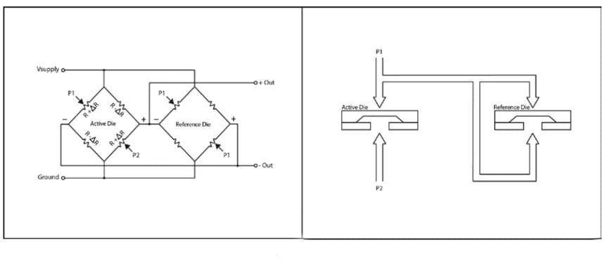
Figure 1 shows the schematic diagram of passive dual-chip compensation.
3. Design and packaging essentials
Turning the dual-chip idea into hardware makes package design, die selection and thermo-mechanical matching crucial. Picking dies from the same wafer and neighbouring positions vastly improves compensation accuracy because temperature coefficients and initial stresses are closely matched. Internal fluid channels in the package must ensure consistent response speed and steady-state behaviour — mismatched channel volumes or impedances create time-constant differences that distort transient responses. Differences in metal terminations, solder and epoxy CTEs (coefficients of thermal expansion) are frequent drift sources; engineers favour low-stress package materials and reduce stress concentrators. You’ll also need to balance front-end amplifier input offsets, resistor matching and filtering to create a front end that corrects bias without amplifying noise. That way the compensated sensor module keeps the sensitivity of a high-precision pressure sensor while improving long-term stability.

Figure 2 illustrates the dual-chip compensation method, which reduces common-mode error compared to traditional methods.
Package size, thermal conduction and long-term drift management
Package size affects thermal distribution and stress paths. Small packages improve thermal uniformity but may limit achievable pneumatic channels; larger packages give more layout room but can introduce temperature gradients. Managing long-term drift starts with material choice, stress isolation and pre-ageing: pick low-stress interface materials, run controlled thermal cycling after packaging to relax stresses, and screen units during production with ageing tests. The front-end circuit’s bias stability and reference supply quality are also essential — good layout and isolation reduce supply-related drift. Combining these measures helps minimise output shifts that develop over time.
4. Calibration and long-term drift management
A dual-chip module needs targeted calibration: zero and span initial calibration, temperature cycling calibration, and accelerated long-term drift testing. Automated calibration rigs can step static pressure and temperature while logging both dies’ responses to compute cross-coupling coefficients. For field use, modules should support self-test and parameter updates, but in high-reliability applications hardware compensation cuts the need for frequent site recalibration. Long-term drift control also requires ageing screening (high temperature, humidity, thermal cycling) and electrical stability checks so high-drift units are culled before shipping. Engineering experience shows properly calibrated, aged dual-chip units often exhibit far lower long-term zero drift than comparable single-chip products.

Figure 3 shows an example of a traditional sensor structure where common-mode error is not reduced.
Pre-heat drift and long-term drift experimental validation
Pre-heat drift stems mainly from internal stress redistribution and circuit stabilisation. Tests typically power the sensor continuously and record output versus time to find the pre-heat time constant and set a stability criterion. Long-term validation uses accelerated ageing — thermal cycling, high-temperature storage, vibration — to evaluate drift under stress. Test rigs gather many runs and statistical data on zero drift, sensitivity change and linearity shifts. Those results let engineers tweak manufacturing or compensation algorithms to boost pass rates and in-field performance.
5. System integration and compensated sensor module implementation
Integrating a dual-chip part into a system requires careful power management, analogue front-end and digital processing co-design. A good compensated sensor module should reduce the host system’s calibration burden while offering a stable digital or standard analogue output. For reliable operation in harsh environments, the module should monitor temperature and supply and raise warnings or step down performance if needed. Integration also needs EMI/EMC, interference rejection and grounding strategies so weak differential signals aren’t compromised. With coordinated hardware and firmware validation, production units can meet both performance and reliability targets.
Linearity improvement and signal integrity optimisation
Dual-chip designs naturally help linearity: averaging two front ends reduces single-side non-linearities and balances positive/negative responses. Signal integrity requires trade-offs across amplifier bandwidth, filter corner frequencies, sample rate and ADC resolution. Over-filtering slows response; under-filtering boosts noise. In practice, staged amplification with mixed low-pass and band-pass filtering and suitable sampling plus digital filtering keeps response times sensible while suppressing noise — making the most of the dual-chip compensation.
Závěr
Dual-chip compensated pressure sensors are an effective route to address micro differential pressure and long-term drift at ultra-low ranges. With matched dies, pneumatic and electrical cross-coupling, precise packaging and strict calibration, system-level drift and common-mode errors can be reduced to a minimum. For designs that need stable, dependable outputs, choosing a compensated sensor module and doing sound power and thermal management at system level cuts maintenance and re-calibration costs. This article walks through the principles and practical steps so engineering teams can decide and implement confidently.
Výše uvedený úvod pouze poškrábe povrch aplikací technologie tlakových senzorů. Budeme pokračovat ve zkoumání různých typů senzorových prvků používaných v různých produktech, jejich fungování a jejich výhod a nevýhod. Pokud byste chtěli více podrobností o tom, o čem se zde diskutuje, můžete se podívat na související obsah později v této příručce. Pokud vás tlačí čas, můžete také kliknout sem a stáhnout si podrobnosti o těchto příručkách Data produktu PDF na tlak vzduchu.
Pro více informací o dalších senzorových technologiích prosím Navštivte naši stránku Sensors.
-e1747998312687.jpg)

